The BGA packaging technology has a series of advantages such as a large number of pins, large IO / terminal pitch (such as up to 1.00 mm, 1.27 mm, 1.50 mm), small inductance and capacitance between leads, and enhanced electrical and thermal performance. Fast, and has been applied in the products of many international famous companies (such as IBM, SUN, Fujitsu, Panasonic, MO TO RO LA, etc.).
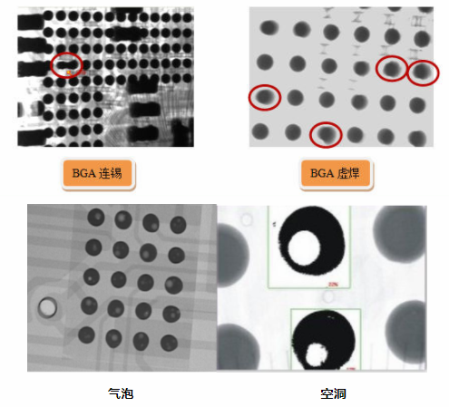
Although the performance of BGA-packaged devices is greatly improved compared to the performance of other packaged devices, since the solder joints of BGA-packaged devices are hidden under the device body, the detection of solder joint defects is more difficult. Under normal circumstances, manufacturers use visual observation to observe whether the collapse of the outermost circle of solder joints is consistent, and then observe the chip facing the light. If each row and each column can pass through the light, it can be preliminary It is determined that there is no bridge, and sometimes larger solder balls can be seen. However, it is difficult to judge whether the solder joint is defective by this method, because it is impossible or difficult to judge whether there are other defects in the solder joint or whether there are voids in the solder joint. In order not to damage the structure and performance of the BGA package device, it can be seen that the internal defects of the BGA package device or the quality of the solder joints can be detected more accurately, other more advanced and reliable non-destructive testing methods must be adopted. For surface-mount solder joints, the most commonly used non-destructive testing method is X-ray inspection. X-ray detectors are used to inspect the solder joints of BGA package devices, which can quickly and accurately detect bridges, voids, and virtual solder joints in BGA package devices And other defects, widely used in the quality inspection of BGA package device solder joints.
There are two types of defect detection problems for BGA packaged devices:
1) Inspection of the BGA package itself. During the production process of BGA packaged devices, solder balls may be lost, solder balls may be too small or too large, solder ball bridges, and solder ball defects may be caused. The inspection of BGA package devices is mainly to check whether the solder balls are missing or deformed.
(2) Inspection of BGA package device assembly solder joints. Mainly check whether there are bridges, open circuits, insufficient solder, lack of balls, blow holes, displacement, etc.

With the emergence of BGA packaging devices and a large number of entering the market, in view of the characteristics of high package density and invisible solder joints, electronic manufacturers need to fully apply high-tech tools and means to control and improve the detection technology in order to control the welding quality of BGAS Level, the use of new process methods can be adapted to the detection methods. Only in this way can the quality problems in the production process be effectively controlled. In addition, the production process is reflected more smoothly and the amount of repairs is reduced.

National Service Hotline
ELT Technology Co., Ltd. All rights reserved
Address: 3rd Floor, Building B, Building 3, Building 2, Guangshen Road, Chaogang Town, Songgang Town, Bao'an District, Shenzhen, China.
Tel: 0755-29411968
Fax: 0755-27330185
E-mail :elt@elt-usa.com
Website: Http://m.szcyprint.com

Wechat Public Number

Mobile website