X-ray inspection technology, commonly referred to as automatic X-ray inspection (AXI), is a technique for inspecting hidden features of a target object or a product that uses X-ray sources. Today, X-ray inspection is widely used in many fields such as medical, industrial control and aerospace. As for PCB inspection, X-rays are used extensively in the PCB assembly process to test the quality of the PCB, which is one of the most important steps for a quality-oriented PCB manufacturer.

Technology advances X-ray
In recent years, area array packages including BGA and QFN, flip chip and CSP are widely used in various fields such as industrial control, communication, military, aviation, etc., making the solder joints hidden under the package. This fact prevents traditional inspection equipment from playing its perfect role in PCB inspection. In addition, due to the appearance of surface mount technology (SMT), which makes packages and leads smaller, traditional inspection methods (including optics, ultrasound, and thermal imaging) are not sufficient because PCBs have higher density and their solder joints Hidden, loopholes or blind holes. In addition, with the increasing miniaturization of semiconductor component packages, the trend of miniaturization of current and future components cannot be ignored while considering X-ray inspection systems. Compared with other inspection methods, X-rays can penetrate into the inner packaging and check the quality of the solder joints. That's why it was picked up.
X-ray inspection principle
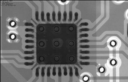
One of the unique advantages of X-ray materials is that they absorb X-rays that are proportional to their atomic weight. All materials absorb X-ray radiation differently according to their density, atomic number, and thickness. In general, materials made of heavier elements absorb more X-rays and are easier to image, while materials made of lighter elements are more transparent to X-rays. Therefore, a general X-ray inspection image is shown in FIG. 1.

From the figure, a dark black image refers to a material composed of heavy elements, and a transparent or relatively white image refers to a material composed of light elements. Therefore, X-ray inspection is a good way to inspect hidden defects, including open circuits, short circuits, misalignments, lack of electrical components, etc.
X-ray inspection technology has brought new changes to production inspection methods. It can be said that it is currently the best choice for manufacturers who are eager to further improve the level of production technology, improve production quality, and will timely find faults in electronic assembly as a breakthrough. With the development trend in the future, other assembly fault detection methods are difficult to implement due to their limitations. X-ray inspection equipment will become the new focus of production equipment in the future, and will play an increasingly important role in the production field!
Established in 2008, Ailante Technology has become a national high-tech enterprise engaged in the research and development of precision X-Ray technology and the research and development of X-Ray intelligent detection equipment. The company's equipment is widely used in electronic manufacturing high-tech industries such as circuit boards, ICs, semiconductors, packaging components, integrated circuits, and LEDs.

National Service Hotline
ELT Technology Co., Ltd. All rights reserved
Address: 3rd Floor, Building B, Building 3, Building 2, Guangshen Road, Chaogang Town, Songgang Town, Bao'an District, Shenzhen, China.
Tel: 0755-29411968
Fax: 0755-27330185
E-mail :elt@elt-usa.com
Website: Http://m.szcyprint.com

Wechat Public Number

Mobile website